
Currently, all of the electronics in my projects are made using copper strip board (vero board). This is great for through-hole components, and larger SMD components, as evidenced in a previous post. However, there are certain components that are not manufacturered in through-hole format. Therefore, the next logical route would be to make a PCB for SMD components.
The journey to get this this point has been far from smooth sailing, as you can see from the numerous failed tests.
Test 1 was use the diode laser with a wave length of 455nm to activate the photo resist on a pre-sensitised board. Test 2 was to try and use an SLA resin printer with a wave length of 395-405nm.
Test 3 was to see if direct sunlight had any effect on the board. As you can see; this didn’t work, and at this point I was starting to feel rather disheartened.
While Tests 4 & 5 look shit; these actually showed hope: something was happening! I could etch, but just not develop. Tests 6 & 7 were successful fails to prove that the developing stage was at fault and to confirm that a caustic was was needed.
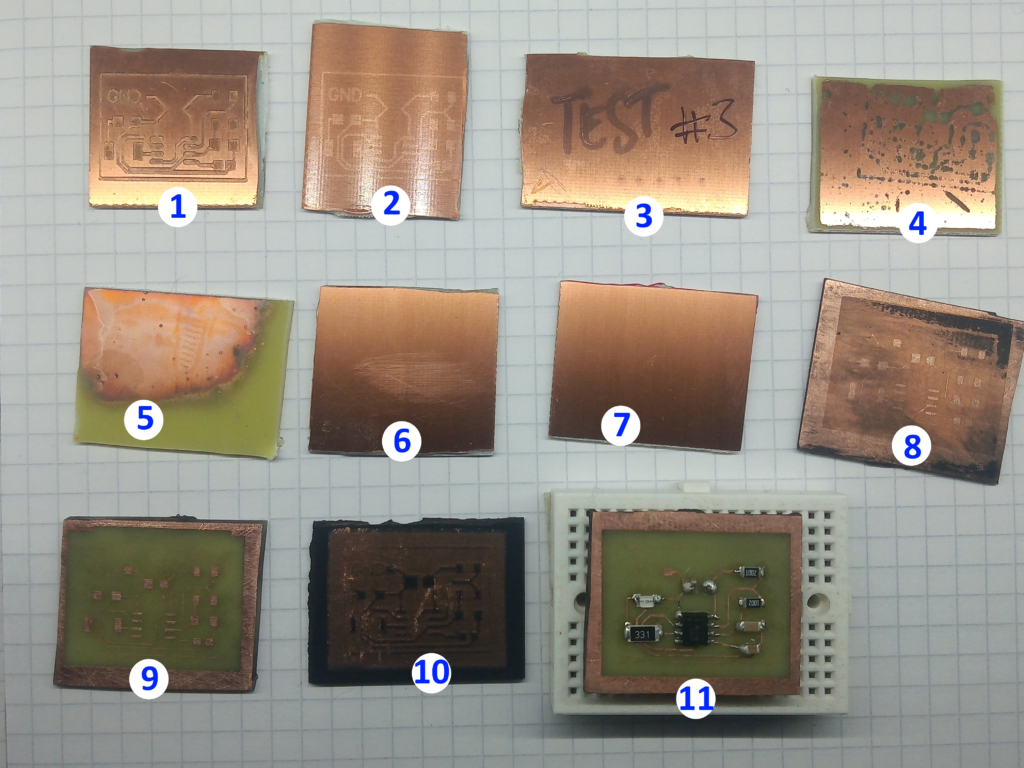
Tests 8 through to 10 were then iterative progressions before a “successful” 11th test. As they say: 11th time’s the charm…
The Method
The inspiration and rough guide came from this video from engineer2you, but tailored to suit my needs.
Parts List:
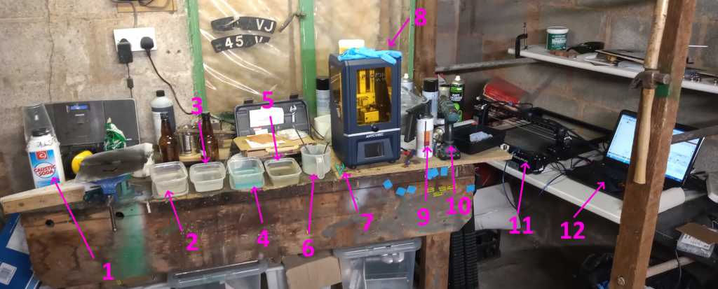
- Caustic soda
- Developer (not used)
- Water bath
- Etch (Sodium Persulphate)
- Caustic bath
- Measuring jug
- Plastic tweezers (not metal)
- Latex gloves
- Black spray paint
- Drill
- Laser diode (10W)
- Computer for laser
Other parts not shown on the photo but required are:
- Blue roll / rag for drying. This shit will bleach, so don’t use your clothes for drying!
- Soft bristled brush
- Safety goggles. You don’t want anything getting in your eyes.
- Dremel cutter for cutting the board. But a hacksaw will work.
- Sandpaper: Greater than 240 grit; ideally around 1200grit. (Apparently a Scotchbrite pad works, too).
- Acetone.
Technique:
The copper board needs to be prepared. As I’m using pre-sensitized board, the top layer needs to be removed. Dip the board in a solution of caustic soda and water (approx 1 table spoon per half pint) and gently rub away the top coating before drying.
Abrade the surface of the copper with a fine grade of sandpaper. This serves as a key for the paint, as well as cleaning the topmost oxide layer. Wipe down with acetone and air dry before spraying with a full, smooth coat of black spray paint: no bare patches, no runs, no drips. (The paint has to be a dark colour for the laser to work).
Meanwhile, prepare your design. For this, I used EasyEDA because as the name states, it was easy. The top layer was exported as a x2.5 scale PNG image. The PNG image was then imported in to LightBurn, scaled down to the correct size and positioned into the correct place.
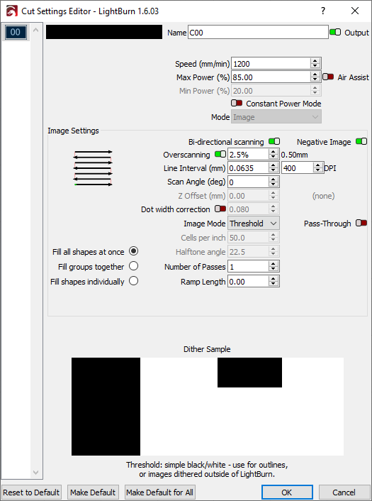
The settings are shown to the right; however the important ones to note are:
- Speed = 1200mm/min.
- Max Power = 85%
- 1 pass at about 400 DPI (greater DPI ≠ better – see Test 9)
- No air assist (see Test 10)
- Default overscanning.
- Negative image with threshold mode.
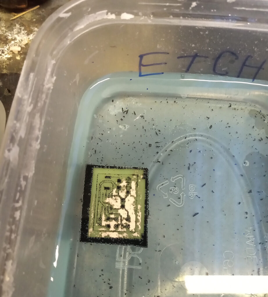
Next is the etching phase. For this, I’m using sodium persulphate. Don’t fuck about with this: use gloves.
Place the still fresh board in the etchant and carefully agitate the container to allow the persulphate to wash over the top.
After a few minutes the lasered paint should be starting to peel from the surface. These flakes of paint need to be gently removed with a brush to expose the copper underneath.
Keep the board in the etchant for as long as it takes to remove the copper; for this small board that time was about 30-45mins.
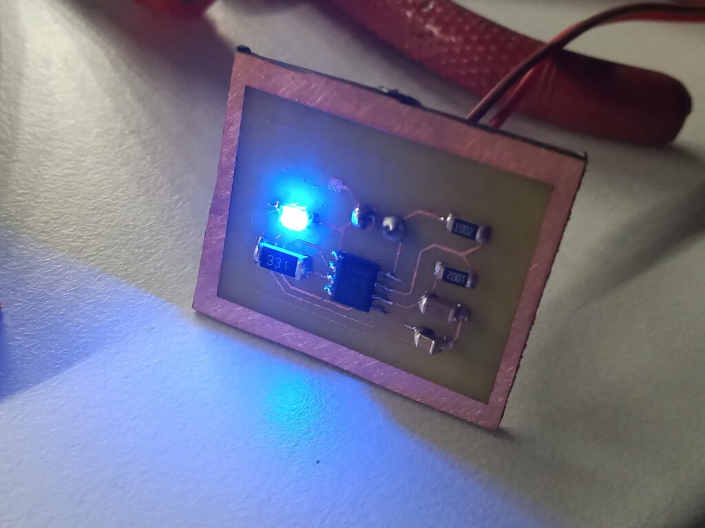
Once the etching has finished, remove the board and clean off the remaining paint with acetone, et voila!
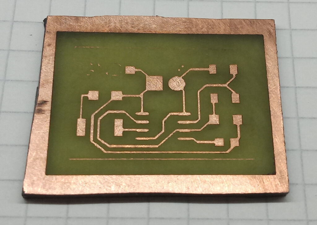
When using this method, make sure your traces are at least 0.50mm wide. Any narrower and there is a high chance of broken circuits (Test 9).
Ultimately, this was just a “for shits and giggles” project as I plan to use a different method of dry photoresist film on copper board, exposed with an SLA printer.